- 您现在的位置:买卖IC网 > Sheet目录1993 > DS1123LE-100+ (Maxim Integrated Products)IC DELAY LINE 256TAP 16-TSSOP
DS1123L
3.3V, 8-Bit, Programmable Timing Element
_____________________________________________________________________
7
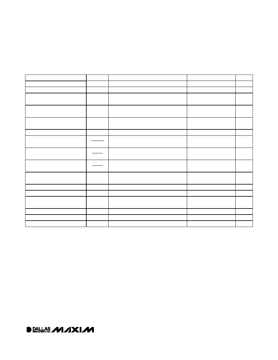
AC ELECTRICAL CHARACTERISTICS (DS1123L-200)
(VCC = +3.0V to 3.6V, TA = 0°C to +70°C.)
PARAMETER
SYMBOL
CONDITIONS
MIN
TYP
MAX
UNITS
Reference Delay
tREF
(Notes 3, 4)
18
22
ns
Delay Step Size
tSTEP
TA = +25°C
1.0
2
3.0
ns
Step-Zero Delay with Respect
to IN
tD0
(Notes 4, 5)
16.5
22
ns
Step-Zero Delay with Respect
to REF
tD0REF
(Notes 6, 7)
-2.5
-1.5
0
ns
Maximum Delay with Respect
to IN
tDMAX
(Notes 4, 8)
527
ns
Delay with Respect to REF
tDREF
Position FF (Notes 7, 9)
510
ns
Delay with Respect to REF
Tolerance
VCC = 3.3V, TA = +25°C
(Notes 7, 9)
-0.75
+0.75
%
Voltage Delay Variation
(Notes 7, 9)
-0.5
+0.5
%
Temperature Delay Variation
VCC = 3.3V
-2.5
+2.5
%
Integral Nonlinearity (Deviation
from Straight Line)
terr
(Note 10)
-5
0
+5
ns
OUT Delta Delay
tINV0
(Note 11)
0
1
2.5
ns
IN High to PWM High
tPWM0
(Notes 4, 12)
16.5
22
ns
Minimum PWM Output Pulse
Width
tPWM
(Note 13)
5
ns
Minimum Input Pulse Width
tWI
(Note 14)
40
ns
Minimum Input Period
(Note 15)
80
ns
Input Rise and Fall Times
tr, tf
(Note 16)
0
1
μs
Note 10:
See the
Integral Nonlinearity section and Figure 9.
Note 11:
Change in delay value when the inverted output is selected instead of the normal, noninverting output.
Note 12:
In PWM mode, the delay between the rising edge of the input and the rising edge of the output.
Note 13:
The minimum value for which the monostable-vibrator pulse width should be programmed. Narrower pulse widths can be
programmed, but output levels may be impaired and ultimately no output pulse is produced.
Note 14:
This is the minimum allowable interval between transitions on the input to assure accurate device operation. This parame-
ter may be violated, but timing accuracy may be impaired and ultimately very narrow pulse widths result in no output from
the device.
Note 15:
This parameter applies to normal delay mode only. When a 50% duty cycle input clock is used this defines the highest
usable clock frequency. When asymmetrical clock inputs are used, the maximum usable clock frequency must be
reduced to conform to the minimum input pulse-width requirement. In PWM mode, the minimum input period is equal to
the step-zero delay and the programmed delay (tDO +tD).
Note 16:
Faster rise and fall times give the greatest accuracy in measured delay. Slow edges (outside the specification maximum)
can result in erratic operations.
Δt
t
DREF
Δt
t
DV
DREF
Δt
t
DT
DREF
发布紧急采购,3分钟左右您将得到回复。
相关PDF资料
DS1124U-25+T
IC DELAY LINE 256TAP 10-USOP
DS1135LU-300/T&R
IC DELAY LINE 300NS 8-USOP
DS1135Z-12/T&R
IC DELAY LINE 12NS 8-SOIC
DS1181LE+
IC CLOCK MOD SS 8-TSSOP
DS1243Y-120
IC NVSRAM 64KBIT 120NS 28DIP
DS1244W-120IND
IC NVSRAM 256KBIT 120NS 28DIP
DS1248Y-70IND
IC NVSRAM 1MBIT 70NS 32DIP
DS1251WP-120+C02
IC NVSRAM 34PWRCP
相关代理商/技术参数
DS1123LE-200
功能描述:延迟线/计时元素 Programmable 3.3V 8 Bit Timing Element RoHS:否 制造商:Micrel 功能:Active Programmable Delay Line 传播延迟时间:1000 ps 工作温度范围: 封装 / 箱体:QFN-24 封装:Tube
DS1123LE-200+
功能描述:延迟线/计时元素 Programmable 3.3V 8 Bit Timing Element RoHS:否 制造商:Micrel 功能:Active Programmable Delay Line 传播延迟时间:1000 ps 工作温度范围: 封装 / 箱体:QFN-24 封装:Tube
DS1123LE-25
功能描述:延迟线/计时元素 Programmable 3.3V 8 Bit Timing Element RoHS:否 制造商:Micrel 功能:Active Programmable Delay Line 传播延迟时间:1000 ps 工作温度范围: 封装 / 箱体:QFN-24 封装:Tube
DS1123LE-25+
功能描述:延迟线/计时元素 Programmable 3.3V 8 Bit Timing Element RoHS:否 制造商:Micrel 功能:Active Programmable Delay Line 传播延迟时间:1000 ps 工作温度范围: 封装 / 箱体:QFN-24 封装:Tube
DS1123LE-50
功能描述:延迟线/计时元素 Programmable 3.3V 8 Bit Timing Element RoHS:否 制造商:Micrel 功能:Active Programmable Delay Line 传播延迟时间:1000 ps 工作温度范围: 封装 / 箱体:QFN-24 封装:Tube
DS1123LE-50+
功能描述:延迟线/计时元素 Programmable 3.3V 8 Bit Timing Element RoHS:否 制造商:Micrel 功能:Active Programmable Delay Line 传播延迟时间:1000 ps 工作温度范围: 封装 / 箱体:QFN-24 封装:Tube
DS1123LS-200
功能描述:延迟线/计时元素
RoHS:否 制造商:Micrel 功能:Active Programmable Delay Line 传播延迟时间:1000 ps 工作温度范围: 封装 / 箱体:QFN-24 封装:Tube
DS1123LS-25
功能描述:延迟线/计时元素
RoHS:否 制造商:Micrel 功能:Active Programmable Delay Line 传播延迟时间:1000 ps 工作温度范围: 封装 / 箱体:QFN-24 封装:Tube